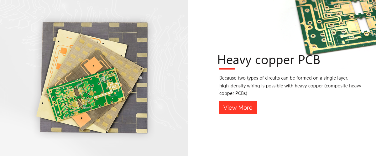
Heavy Copper PCB
2020-03-23Heavy Copper PCB
All Printed Circuit Boards (PCB) are constructed to carry current through the copper traces etched on to the different layers. In today's applications where current density, economics, and size plays a vital role, increasing the width of current traces to accommodate a higher current is not a viable option available to designers. The best solution to this dilemma is the use of heavy Copper PCB, where the thickness of copper traces is increased, keeping the width constant. The result is the increase in the current-carrying and heat dissipation capacity of the components present in the PCB system.
Heavy Copper PCB has no standard definition but forms a crucial part of high Power Applications where a copper thickness of 3 oz ft2 to 20 oz ft2 is required in inner or outer layers. Most ordinary PCB manufactured have a copper thickness of 1/2 oz - 3 oz ft2. Devices that require a copper thickness of over 20 oz ft2 are categorized as Extreme Copper PCB.
Heavy Copper PCBs are extensively used in the Power Electronics and Power Supply systems where there is a high current requirement or a possibility of quick shooting up of fault current. The increased copper weight can turn a weak PCB board into a solid, reliable, and long-lasting wiring platform and negates the need for an added costlier and bulkier components like Heat sinks, fans, etc.
Benefits of using Heavy Copper PCBs
- Increased Endurance to thermal stress
- Elimination of complex wired bus configuration
- Optimized for use with high-temperature materials with a lower circuit failure rate
- Strong and uncomplicated structure with lowered layer count and smaller Footprint
- Lower Production costs as it replaces thick copper cables
- Enhanced Current carrying capacity and assisted transferring of current to the exterior Heat sink through heavy copper plated vias
- Improved Mechanical Strength in Connector Sites and PTH holes
- On-board high Power density for Planar Transformers
Design Considerations for Heavy Copper PCBs
The current carrying capacity and maximum permissible conductor temperature of the PCB depends primarily on the width and thickness of the heavy copper. The copper thickness to be used should be determined during the circuit design process by the amount of rated current in the circuit, Also, the designer needs to take care of the heat dissipation. As current flows through the copper traces, its resistance heats up the track and requires a heat dissipation unit for dissipating the power generated into the surroundings. The maximum current decides the size of the trace as we need to dissipate the heat before it crosses the acceptable temperature rise of around 30C.
Few other design considerations include the Substrate material of PCB and Thermal Coefficient of Expansion (TCE) between the heavy copper and substate material of the PCB. This is prominent as the thermal stress due to high current can cause cracks and layer separation, eventually driving the PCB to failure,
Heavy Copper PCBs Fabrication
Any PCB manufacturing, whether single-sided or double-sided is composed of copper etching to remove the unwanted copper and plating techniques to add thickness to the planes, pads, and traces and Plated-Through-holes (PTH). The Fabrication of Heavy Copper PCBs is quite similar to the construction of regular FR-4 PCBs but they require special etching and electroplating techniques which increases the thickness of the surface board without altering the layer count. The thick Surface Boards are capable to handle added copper weights due to the specialized techniques that involve high-speed, self plating, and differential or deviation etching.
The normal etching method does not work for Heavy Copper PCBs and creates uneven edge lines and over-etched margins. We use advanced plating techniques to obtain Straight lines and optimal edge margins with negligible undercuts. Our process of additive plating decreases the resistance of copper traces thereby enhancing the heat-conducting capacity and endurance for thermal stress.
The Reduction in thermal resistance improves the heat dissipation capacity of your circuit through thermal convection, conduction, and radiation. Our Fabricators are also focused on thickening the walls of PTH which serves numerous advantages by shrinking the layer count and reducing impedance, foot-print, and overall manufacturing cost. We take great pride in being one of the most affordable and quality Heavy Copper PCBs manufacturers around the globe.
However, these PCBs involves higher cost than regular PCBs as the etching process is vigorous and difficult. Huge amounts of Copper need to be eliminated during the Etching process. Also, the lamination process demands the utilization of Prepreg with high resin content for filling the spaces between the copper traces. So, the cost of manufacturing is higher than Regular PCBs. Nevertheless, we employ a combination of Blue Bar Method and Embedded Copper method for providing you a superior board at the best price.
Application of Heavy Copper PCBs
We often manufacture and supply these PCBs where there is frequent or sudden exposure to excessive current and augmented temperature. Such extreme levels are enough to damage a regular PCB and call for Heavy Copper requirement which also lowers the layer count, offers lower impedance, and enables smaller footprint and huge cost savings. Below are few industries and applications that we cater to for Heavy Copper PCBs:
- Power Distribution systems
- Power Amplifier Modules
- Planar Transformers
- DC-Tp-DC Power Converters
- Automotive Power Distribution Junction Boxes
- Power Supplies for Radar Systems
- Welding Equipment
- HVAC Systems
- Nuclear Power Applications
- Protection and Overload Relays
- Railway Electrical Systems
- Solar Panel Manufacturers, etc.
In recent years, the demand for these PCBs has escalated in Automotive, Military, computer, and industrial control applications. We at Golden Triangle Group have decades of experience in delivering Heavy Copper PCBs of supreme quality. Our Skilled Engineers are devoted to meet the highest standards and create Premium Boards that meet your performance expectations and profitability goals. We understand that Heavy Copper PCB designing comes with additional complexities and hence, we closely address all questions and concerns before proceeding with the production.
What makes us special is that our developed boards pass through various cycles of quality check before it is delivered to our clients. Our in-house quality control department guarantees the quality of the Heavy Copper PCBs and makes sure that the final product meets the finest quality with minimal to no risk of circuit failure.
